![[Return to Physics Homepage]](./../../physics.gif)
![[Return to Mike Coombes' Homepage]](./../../coombes.gif)
![[Return to List of Handouts]](./../../handouts.gif)
![[Return to Problem Sets]](./../../problems.gif)
![[Return to List of Solutions]](./../../solutions.gif)
Questions: 1 2 3 4 5 6 7 8 9 10
A transistor is in saturation when IC £ βDCIB. To determine the saturation status, we first get Kirchhoff's equations for the transistor.
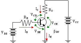
Our equations are
| (1) | |
| (2) | |
| (3) |
From equation (2), we can determine IB = (VBB - VBE)/RB. From equation (3), we can determine Ic(sat) for the given value of VCE (sat), IC(sat) = (VCC - VCE(sat))/RC. If IC(sat) £ βDCIB, then the transistor is in saturation.
Using EXCEL, we can write a spreadsheet that answers the question automatically.
|
|
|
|
|
|
|
|
|
|
|
|
|
|
|
|
|
|
|
|
|
|
|
|
|
|
|
|
|
|
![[Return to Top of Page]](./../../top.gif)
As noted in question 1 above, we determine IC(sat) by
From
we see that we are free to adjust VBB to get any value of IB. If we increase VBB, we increase IB and the product βDCIB. Saturation occurs when βDCIB ³ IC(sat). Hence the transistor will be in saturation when IB ³ IC/βDC. The minimum value of IB which causes saturation is therefore
Substituting the value of IB(sat) given by equation (3) into equation (2), we find the minimum value of VBB that causes saturation to be
Again using EXCEL, we can write a spreadsheet that answers the question automatically.
|
|
|
|
|
|
|
|
|
|
|
|
|
|
|
|
|
|
|
|
|
|
|
|
|
The Q-point is a point on a graph of IC versus VCE. Assuming that the transistor is neither in saturation or cutoff, the value ICQ is found from ICQ = βDCIB, where IB is determined by the equation IB = (VBB - VBE)/RB derived in question 1. The value of VCEQ is found by using ICQ and equation (3) from question 1, VCEQ = VCC - ICQRC .
To answer the rest of the question, we need to examine the "DC Load line". The load line is the line drawn on the IC versus VCE graph that runs from the saturation point (IC(sat), VCE(sat)) to the cutoff point (IC(cutoff), VCE(cutoff)). As we have seen, we get IC(sat) from IC(sat) = (VCC - VCE(sat))/RC. The cutoff occurs when IC = 0. This implies VCE(cutoff) = VCC.
Using Excel to determine each Q-point, saturation point, and cutoff point yields
|
|
|
|
||||
|
|
|
|
|
|
|
|
|
|
|
|
|
|
|
|
|
|
|
|
|
|
|
|
|
|
|
|
|
|
|
|
A sketch of the DC Load line is useful
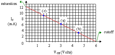
Note that increasing IB will move a Q-point toward saturation while decreasing it will move the Q-point toward cutoff. Now Ib is the AC signal that is added to IB. The variation in the sum of IB + Ib has the same effect as increasing or decreasing IB; that is if Ib has too large a peak value the transistor will be driven into saturation or cutoff. Examining the graph, we see that the Q-point for part (a) is in the middle of the graph. As the peak value of Ib, Ib(peak), increases, it simultaneously enters both cutoff and saturation. The value of Ib(peak) that this occurs at is
or
whichever is smaller. For part (a), both equations give the same result since ICQ is equidistant to both the saturation and cutoff points. For part (b), ICQ is closer to cutoff so equation (2) is the appropriate one to choose. For part (c), ICQ is closer to saturation so equation (1) is the appropriate one to choose. Calculating Ib(peak) yields
|
|
|
|
|
|
|
|
|
|
|
|
|
|
|
|
First we apply Kirchhoff's rules to the transistor
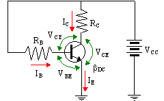
and derive the equations
| (1) | |
| (2) | |
| (3) |
We get the Q-point as follows. We find IB from equation (3), IB = (VCC - VBE)/RB. Assuming that we are not in saturation, we get ICQ = βDCIB. Then using equation (2), we find that VCEQ = VCC - ICQRC. As in question 3, the saturation point occurs when IC(sat) = (VCC - VCE(sat))/RC. The cutoff occurs when IC = 0, or VCE(cutoff) = VCC.
Using Excel to calculate these quantities, we find
|
|
|
|
||||
|
|
|
|
|
|
|
|
|
|
|
|
|
|
|
|
|
|
|
|
|
|
|
|
|
|
|
|
|
|
|
|
The graph of the load line for these points looks like
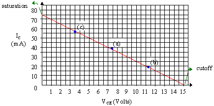
Note that increasing IB will move a Q-point toward saturation while decreasing it will move the Q-point toward cutoff. Now Ib is the AC signal that is added to IB. The variation in the sum of IB + Ib has the same effect as increasing or decreasing IB; that is if Ib has too large a peak value the transistor will be driven into saturation or cutoff. As shown in question 3, the values of Ib(peak) that this occurs at are Ib(peak) = (IC(sat) - ICQ)/βDC or Ib(peak) = (ICQ - IC(cutoff))/βDC, whichever is smaller.
For part (a), both equations give the same result since ICQ is slightly closer to saturation. For part (b), ICQ is closer to cutoff . For part (c), ICQ is closer to saturation. Calculating Ib(peak) yields
|
|
|
|
|
|
|
|
|
|
|
|
|
|
|
|
First we apply Kirchhoff's rules to the transistor
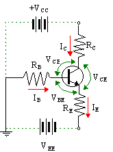
and derive the equations
| IC + IB = IE | (1) |
| VCC - ICRC - VCE - IERE + VEE = 0 , | (2) |
| -IBRB - VBE - IERE + VEE = 0 . | (3) |
This set of equations is more complicated than the sets we had for the prior bias circuits. Nonetheless the equations may be solved. First we assume that the transistor is neither in saturation, so that IC = βDCIB and IE = (βDC+1)IB. Equation (3) then yields an expression for IB
Replacing IC and IE in equation (2) to get an equation for VCE yields
Note that both equations (4) and (5) depend on VEE, that is that a particular value of VEE determines a value for IB which in turn sets the value of VCE - provided that the system is not in saturation.
To determine the saturation point, we need to first find the value of VEE(sat). Using equation (4) to eliminate IB from equation (5) yields,
or, collecting like terms
 .
(6)
.
(6)Rearranging the above to find VEE gives
 .
(7)
.
(7)Setting VCE = VCE(sat), we get the value of VEE(sat), which we can substitute back into equation (4), do some algebraic manipulation, and get IB(sat),
Off course, just at saturation IC(sat) = βDCIB(sat),
The cutoff occurs when IB = IC = IE = 0. From equation (4), we see that IB = 0 if and only if VEE = VBE. So for cutoff,
Using Excel to calculate these quantities, we find
|
|
|
|
||||
|
|
|
|
|
|
|
|
|
|
|
|
|
|
|
|
|
|
|
|
|
|
|
|
|
|
|
|
|
|
|
|
|
|
|
|
|
|
|
|
There are several important points to draw from these results. The first is that for a given value of RE, the Q-point does not vary very much with βDC. We say that the Q-point is stable. This is important in a circuit since βDC is strongly temperature dependent; in an emitter bias circuit the output will not fluctuate with temperature. The second is that RE can be adjusted to determine the Q-point. The last point is that changing either βDC or RE does not effect the cutoff and has only a small effect on the saturation point. As a result, we can draw one load line for all the points. The graph of the load line for these points looks like
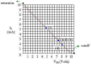
Note that increasing IB increases IC which will move a Q-point toward saturation while decreasing it will move the Q-point toward cutoff. Now Ib is the AC signal that is added to IB. The variation in the sum of IB + Ib has the same effect as increasing or decreasing IB; that is if Ib has too large a peak value the transistor will be driven into saturation or cutoff. As shown in question 3, the values of Ib(peak) that this occurs at are Ib(peak) = (IC(sat) - ICQ)/βDC or Ib(peak) = (ICQ - IC(cutoff))/βDC, whichever is smaller.
Examining the graph of the load line, we see that the signal will first go into cutoff for parts (a), (b), and (d) while the signal will go into saturation for (c). Calculating Ib(peak) yields
|
|
|
|
|
|
|
|
|
|
|
|
|
|
|
|
|
|
|
|
We saw in Question 5, that adjusting RE moves the Q-point around. In this question, we are asking what value of RE will cause VCE to equal VCE(sat). If we take equation (6) form Question 5,
we need to rearrange this equation to determine RE when VCE = VCE(sat). After a good deal of manipulation, we arrive at

Using Excel to calculate the results yields
|
|
|
|---|---|
|
|
|
|
|
|
|
|
|
First we apply Kirchhoff's rules to the transistor
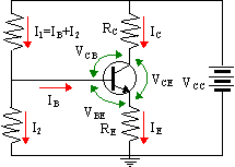
and derive the equations
| IC + IB = IE | (1) |
| I1 = IB + I2 | (2) |
| VCC - ICRC - VCE - IERE = 0 | (3) |
| VCC - I1R1 - I2R2 = 0 | (4) |
| I2R2 -VBE - IERE = 0 | (5) |
We get the Q-point as follows. First we assume that we are not in saturation, so that IC = βDCIB and IE = (βDC+1)IB and make this substitution into the Kirchhoff equations above. Next we eliminate I2 leaving
| VCC - VCE - IB[βDCRC + (βDC+1)RE] = 0 | (1) |
| VCC - IB[R1 + (βDC+1)RE(R1+R2)/R2] - VBE(R1+R2)/R2 = 0 | (2) |
Then we find IB from equation (7)
This result may be used with
to uniquely determine the Q-point.
Cutoff, the point when IB = IC = IE = 0, will occur when the value of R2 is such that equation (7) becomes
The value of R2(cutoff) which meets the above criterion is
The value of VCE(cutoff) can be seen from equation (6) to be
The saturation point can be found from equation (9)
and IC(sat) = βDCIB(sat).
Using Excel to calculate these quantities, we find
|
|
|
|
||||
|---|---|---|---|---|---|---|
|
|
|
|
|
|
|
|
|
|
|
|
|
|
|
|
|
|
|
|
|
|
|
|
|
|
|
|
|
|
|
|
There are several important points to draw from these results. The first is that for a given value of R2, the Q-point is stable and hardly changes with βDC. It changes even less than the two battery bias of Question 6. This is important in a circuit since βDC is strongly temperature dependent; in a voltage divider bias circuit the output will not fluctuate with temperature. The second is that R2 can be adjusted to determine the Q-point. The last point is that changing either βDC does not effect the cutoff and has only a small effect on the saturation point. As a result, we can draw one load line for all the points. The graph of the load line for these points looks like
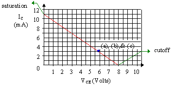
Note that increasing IB increases IC which will move a Q-point toward saturation while decreasing it will move the Q-point toward cutoff. Now Ib is the AC signal that is added to IB. The variation in the sum of IB + Ib has the same effect as increasing or decreasing IB; that is if Ib has too large a peak value the transistor will be driven into saturation or cutoff. As shown in question 3, the values of Ib(peak) that this occurs at are Ib(peak) = (IC(sat) - ICQ)/βDC or Ib(peak) = (ICQ - IC(cutoff))/βDC, whichever is smaller.
Examining the graph of the load line, we see that the signal will first go into cutoff for all three parts (a), (b), and (c). Calculating Ib(peak) yields
|
|
|
|
|---|---|---|
|
|
|
|
|
|
|
|
|
|
|
|
If we examine equations (8) and (9) from Question 7,
we see that changing R2 changes IB. Thus we can find a value of R2 that causes VCE to equal VCE(sat). To find R2(sat), we eliminate IB from the second equation using the first. Then we work through the algebra to isolate R2. After a good deal of algebraic manipulation we find

Using Excel to calculate the results yields
|
|
|
|---|---|
|
|
|
|
|
|
|
|
|
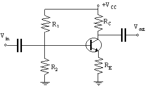
The AC internal resistance of the transistor from Base to Emitter is given by the formula
To find IE, we use the equations developed in Question 7 to find the Q-point. We can do this because the capacitors block DC signals; in DC the above diagram is simply a Voltage Divider biased transistor. Using Excel to do the calculations, we find
|
|
|
|
|
|
|
|
|
|
|
|
|
|
|
where we have used βDC = β , i.e. we assumed that the DC and AC current gain are equal.
For the other quantities we are looking for, we need to consider what the circuit looks like in AC. Some points to note. In AC capacitors act as shorts if XC is small. The DC source VCC act as a ground in AC. The input Vin, or source signal, has a resistance RSource. The output resistance Vout also may have a load resistance, Rload. The transistor may be considered to a combination of two resistors, re and rc. As mentioned re is the base-emitter resistance which is usually small while rc is the base-collector resistance and is huge in the order of megaohms. The resistance of rc is huge because in that direction the transistor is like two reverse-biased diodes in series. The circuit will look like
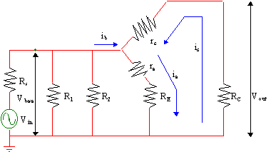
The quantity Rin(base), the effective resistance of the emitter branch, is defined as the voltage at the base divided by the base current
Rin(base) is the effective resistance of the emitter branch because the base-collector junction is a reverse-biased diode and thus can be treated as an open as shown below
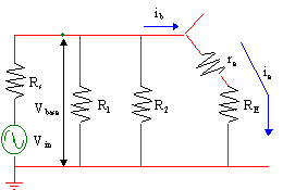
It's not quite that simple since we have Ib entering the emitter branch but the potential drop is much greater than Ib(re+RE) as we have seen. "Looking into the base" the resistance of the arm appears to be Rin(base). In a similar fashion, the total resistance of the transistor circuit as seen by input voltage is the effective resistance of the three parallel branches in the diagram above which is denoted Rin and
Rin is connected in series with the source and its resistance. Thus the potential at the base in terms of Vin is
The quantity An is the voltage gain, the ratio of the output voltage to the base voltage, defined
The quantity An ' is also a voltage gain but is the ratio of the output voltage to the input voltage
Using Excel, we find the following numerical results
|
|
|
|
|
|
|
|
|
|
|
|
|
|
|
|
|
|
|
|
|
Bypassing a resister by a capacitor means to short it out to AC signal. In DC there is no effect as a charged capacitor act as an open. Thus Q-point would not be affected effected. The effect is to set RE to zero in our equations in Question 9 above. In AC, the first effect of the bypass capacitor would be to change Rin(base) and Rin. Recall that without the bypass Rin(base) = Ib(re+RE) but RE is now zero so
This in turn alters the value of Rin since Rin = R1||R2||Rin(base).
Following on through the derivations in Question 9, the voltage gain An , the ratio of the output voltage to the base voltage, becomes
The quantity An ', is unchanged except for the value of Rin
Redoing the calculations yields
|
|
|
|
|
|
|
|
|
|
|
|
|
|
|
|
|
|
|
|
|
Questions? mike.coombes@kpu.ca
![[Return to Kwantlen Homepage]](http://www.kpu.ca/images/return_button.gif)